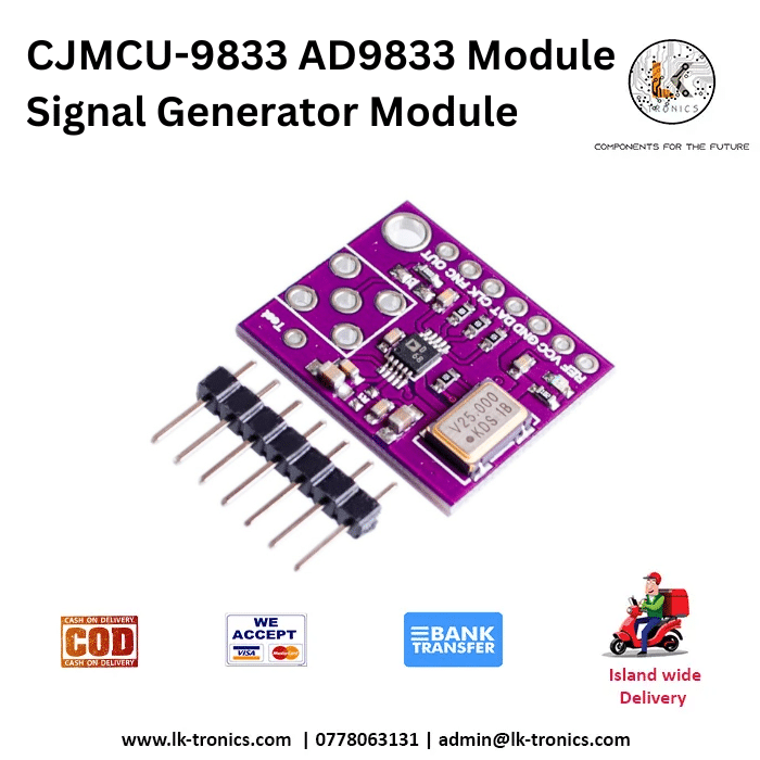
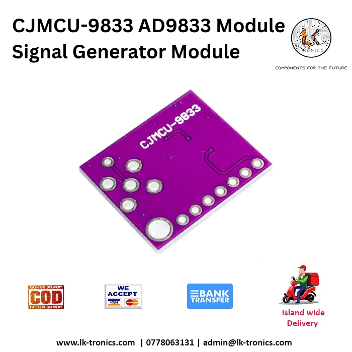
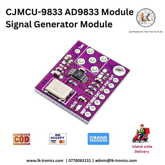
CJMCU-9833 AD9833 Module Signal Generator Sine Square Triangle wave Module
The AD9833 Module Signal Generator is a versatile and compact device that allows for the generation of various types of signals. With its high precision and stability, it is suitable for a wide range of applications including audio testing, frequency synthesis, and waveform generation. The module features a programmable frequency range, allowing users to generate signals from 0.1 Hz to 12.5 MHz with a resolution of 0.1 Hz. It also offers a programmable phase control, enabling precise phase adjustments for signal synchronization. With its user-friendly interface and easy-to-use controls, the AD9833 Module Signal Generator is an essential tool for engineers, researchers, and hobbyists in need of a reliable and efficient signal generation solution.
The AD9833 Function Generator Module is a frequency programmable sine, triangle, and square wave generator with an SPI interface.
FEATURES:
- 0-12.5MHz output frequency range
- 0.1Hz resolution
- 10-bit digital-to-analog output converter
- sine, triangular, and square waveform outputs
- Simple and complex modulation capability
- Phase control
- 3-wire SPI interface
- 3.3V and 5V logic compatible.
The AD9833 function generator can be used to provide various signals for electronic testing by serving as a function generator and it can be used in various sensing, actuation, and time-domain reflectometry (TDR) applications such as for testing cables or FSK or other keying application.
Powering the Module
The module can operate from 2.3 to 5.5V and so is compatible with both 3.3 and 5V MCUs.
Internally, the AD9833 contains a 2.5V regulator and operates at 2.5V. If you want to operate the module at a VCC voltage < 2.7V, the location on the board mark R1 which is normally open should be shorted so that VCC is connected directly to the CAP2.5V input which bypasses the internal regulator.
A red LED illuminates when power is appli to the module.
Waveform Output
The AD9833 can be programm to output either a sine, triangular or square wave. When the module is first powered up, it automatically outputs a default 1kHz sine wave.
Sign Wave
The AD9833 creates sine waves by the use of a numerically controlled oscillator, phase modulator, sin look-up ROM, and DAC.
The output DAC is a high-impedance 10-bit current source DAC. A built-in 200-ohm load resistor converts the current to a 0.6Vp-p voltage output that swings between ground and about +0.6V. At frequencies above 1MHz, the signal amplitude starts decreasing.
Triangle Wave
When the triangle waveform is select, the sin look-up ROM is bypassed and the output of the NCO is sent directly to the on-chip DAC which provides a 10-bit triangular output. The triangle wave output will also be approximately 0.6Vp-p up to 1MHz and then start to decrease at higher frequencies.
Square Wave
The square waveform is creat by just sending the MSB (Most Significant Bit) of the DAC data to the output. Unlike the other two waveforms, the square wave output is a logic level and will swing the full range from ground to Vcc over most of its range.
Connecting to the output
The output of the AD9833 is available in 3 places. On the header pin mark ‘OUT‘, on the center pin of the unstuffed BNC connector location which is surrounded by 4 ground pins, and at the pad marked ‘Tset‘.
The output of the module is not a buffer. Depending on the applications, it may be desirable to add an op-amp or similar buffer on the output to modify the levels and/or add drive capability. The output has a series resistor and capacitor location on the board. As shipped, the resistor location is stuffed with a 0-ohm resistor. The larger C2 capacitor location next to it is unstuffed. If it is desired to AC couple the module, the 0-ohm resistor can be removed and a capacitor can be added to C2.
SPI Interface
The module has an easy-to-use 3-wire SPI interface that uses Data (SPI MOSI), Clock (SPI CLK), and Load (SPI SS) which is call FSYNC on the AD9833.
Module Assembly
This module comes with the header loose. This allows you to configure the module to meet your particular requirements such as which side of the board you want the header on or if you want to solder on wires to make the connections.
For use with breadboards, we put the headers on the bottom so that the module can plug directly into the breadboard.
If you are working with the module using an O’scope, you may find it handy to add a header pin to the Tset location for hooking up a scope probe. For some applications, such as building a little function generator, you may want to add a 5-pin BNC connector to the module to allow hooking up to BNC-shielded cables
Module Connections
The connections to the module are fairly straightforward.
Supply 3.3 or 5V power and ground from the MCU
Connect the 3 SPI pins to the SPI pins on the MCU. The location of these pins will depend on which module you are using
Hookup a scope to the output to see what the generator is doing
1 x 7 Header
REF = 25MHz Reference clock from the onboard oscillator is output on this pin.
VCC = Vcc power (2.3 to 5.5V)
GND = Ground
DAT = SPI Bus Data pin (MOSI)
CLK = SPI Bus Clock pin
FNC = SPI Bus Load pin (SS) (called FSYNC on the AD9833)
OUT = Output of the function generator. Also available on the center pin of the BNC location and set
VISIT OUR FACEBOOK PAGE FOR MORE INFO | MORE PRODUCT IN OUR SHOP
Based on 1 review
Add a review
You must be logged in to post a review.


Tharaka Gamage –
Rare product find in Sri lanka.nicely working.thank you
Tharaka Gamage –